(For LE-8200A/8200)
OP-SB85L
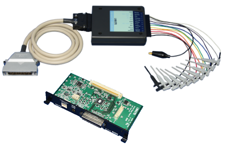
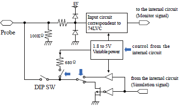
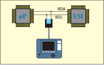
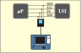
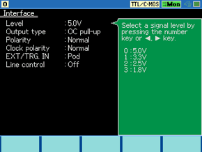
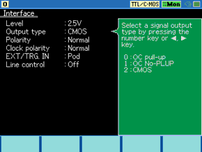
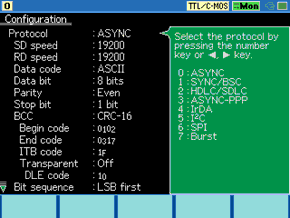
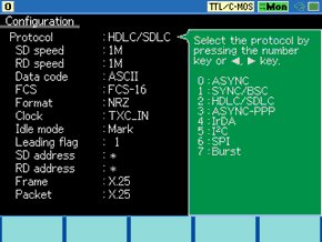
OP-SB85L is the interface expansion kit that has a port to measure TTL / CMOS signal level communications, and the one to measure the voltage of high-speed analog input. The port for TTL / CMOS supports the measurement of TTL / CMOS level communications that power supply system is from 1.8V to 5V. It is suitable for monitoring the communication between the LSI and the interface IC on the printed circuit board by directly probing into the lines. It supports the protocol of not only UART and HDLC but also I2C and SPI on monitoring and simulating.
Furthermore, it has BURST measuring mode that captures data at all clock edges.
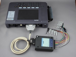
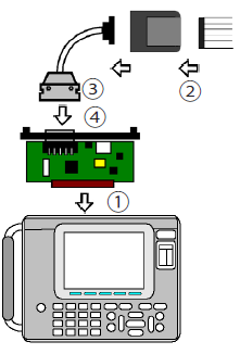
[ OP-SB85L set to LE-8200A ]
[ OP-SB85L and its probe pod&unit ]
Operating Instructions
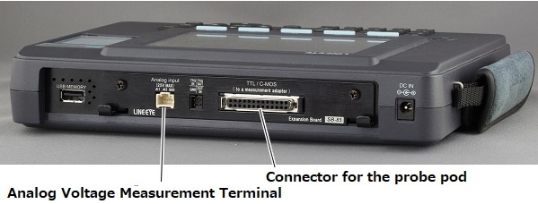
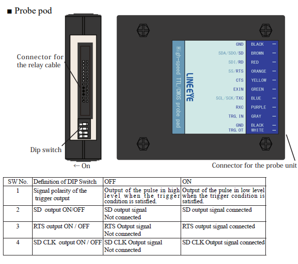
After inserting the expansion board into an analyzer (LE-8200A/LE-8200), connect the communication lines to measure, using the included probe pod. Since 9 kinds of signal lines can be tested, you can measure various communications: SD(SDA/SDO), RD(SDI), RTS(SS), CTS, EXIN, TXC(SCL/SCK), RXC, trigger input and trigger output. Moreover, you can set the polarity of data and the clock you wish to capture.
Monitor function
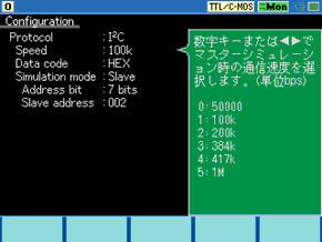
Normal mode (USART) allows to use all functions such as trigger function. BURST mode allows to measure clock SYNC which is not supported in former models. (Clock SYNC: clock is given only when transmitting data.) I2C mode allows to measure I2C serial communications with start/ stop sequence. I2C and SPI communications can be displayed in translation display and it is possible to analyze read and write sequence.
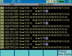
■I2C
This kit can test the I2C serial communication including start sequence and stop sequence by setting I2C mode.
I2C and SPI mode have the translation display and analyze the read and write sequence efficiently.
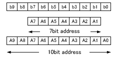
The relation of input data and address is as follows.
e.g.) Input “123”;
[If 7 bit] "0010001" is set.
[If 10 bit] "0100100011" is set.
| Display | Meaning |
|---|---|
| Time/ ΔTime |
It displays the time of receiving data./ It displays the difference of time. (Switchable by pressing [F5]) |
| → | Indicates the transmission (write) from Master. |
| ← | Indicates the reception (read) from Master. |
| Adress/ Data |
Indicate the slave address and data in HEX. |
| [01] | Indicates the non-acknowledge. |
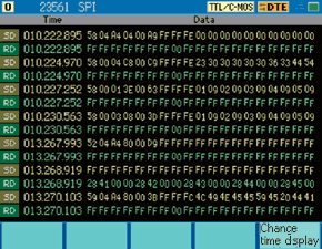
■SPI
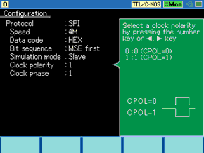
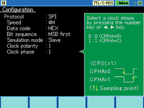
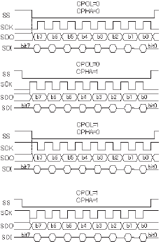
The timing of clock and data set at “CPOL” and “CPHA” is described in above figure.
| Time/ ΔTime |
It displays the time of receiving data./ It displays the difference of time. (Switchable by pressing [F5]) |
|---|---|
| Data | It displays data in HEX. |
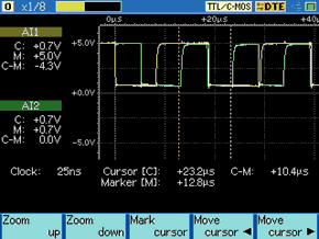
Analog Waveform Analysis
It displays the waveforms at a sampling rate up to 40M for 2 channels and supports ±12V. This function helps to identify hardware problems. You can also use it for educational purpose for people studying data communications.
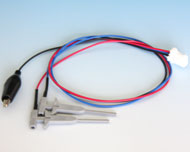
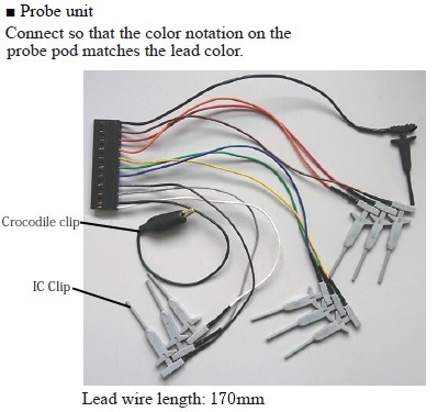
A probe cable with test clips is attached.
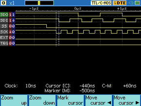
Digital Waveform Measurement (Logic Analyzer) Function
Logic Analyzer function analyzes timing between data signal and clock signal on I2C/SPI of max at 100MHz sampling.*1
Simulation / BERT
Excepting the BURST mode, using the simulation function enables you to vastly enhance the efficiency of the development and the trouble analysis. In the I2C and SPI mode, you can simulate in both the master and the slave. Also, since the bit error rate test (BERT) is available in the normal mode (USART), you can easily test the transmission feature of the device, etc.