OP-SB5GL
Also, as it has a probe for TTL level transmit/receive clock, it can monitor USART synchronous communication. In addition to general UART and HDLC communication measurements, it supports monitoring and simulationion of I2C, SPI, and monitoring of Burst mode which captures all data in synchronization with the clock.
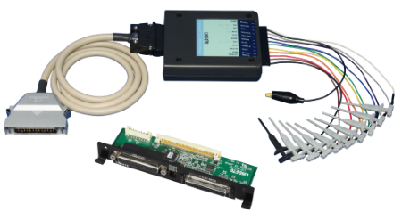
Applicable analyzers: LE-3500XR(V2), LE-2500XR(V2), LE-3500XR, LE-2500XR, LE-3500R, LE-2500R, LE-1500R, LE-3500, LE-2500, LE-1500[ OP-SB5GL set to LE-2500XR ]
[ OP-SB5GL set to LE-3500XR ]
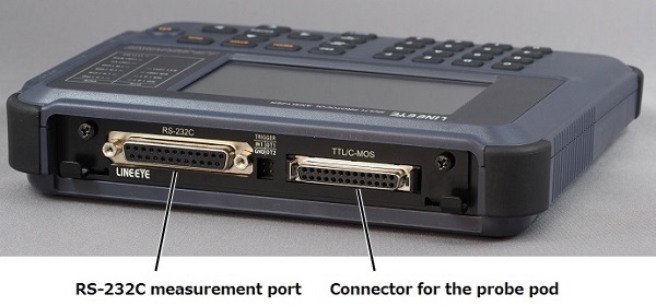
Operating Instructions
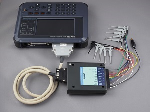
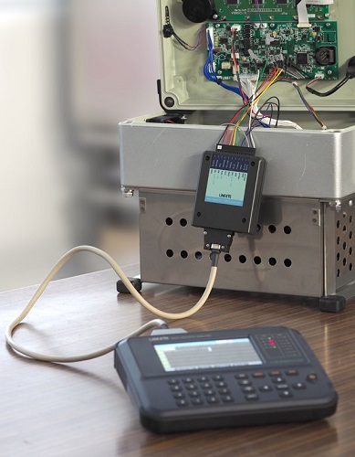
After inserting the expansion board into the analyzer, clip the communication line you want to measure using the attached probe pod.
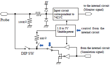
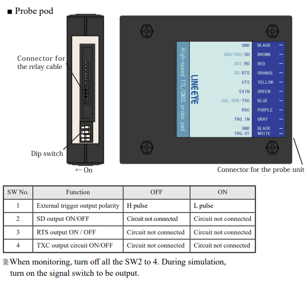
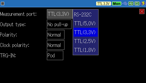
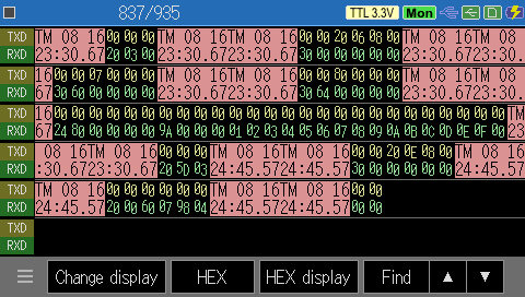
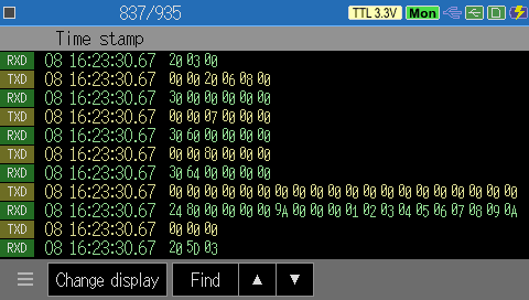
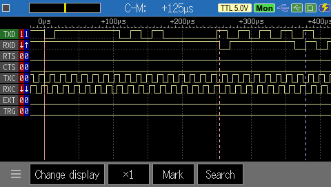
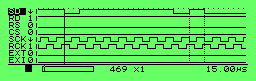
SD, RD, RTS, CTS, EXIN (external signal input), TXC (SD_CLK), RXC (RD_CLK), TRG.IN (external trigger input), and TRG.OT (external trigger output) signal lines can be monitored. It also supports communication with external clock of TTL level. You can also set the polarity of the data and the polarity of the clock to be fetched.
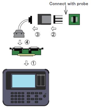
As it can be connected by the relay cable from the target to the probe which has a built-in signal receiver, it can be used for a large test objects.
Monitoring
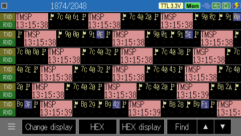
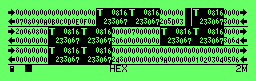
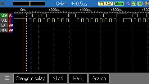
In the normal mode (USART), you can make full use of the functions of an analyzer such as the trigger function. Also, by setting the BURST mode on the analyzer, you can measure communication system (clock synchronous communication) which supplies the clock at the time of only transmitting data. That makes it possible to monitor communication that the old protocol analyzers cannot measure.
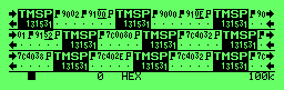
Example of Clock Synchrounaous Communication
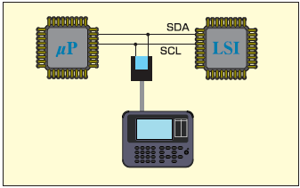
■I2C
By setting the I2C mode, you can test the I2C serial communications including the start sequence and stop sequence. Since the translation display is available in I2C, you can efficiently analyze the sequences of Read and Write.
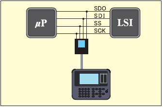
■SPI
By using LE-3500XR/LE-2500XR/LE-3500R/LE-2500R, it can monitor SPI communications, which is widely used in transferring communications. Refer to the SPI additional specificationfor details.
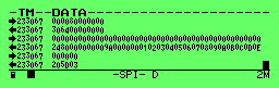
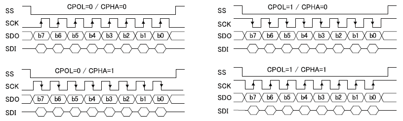
It supports all four SPI transfer timings by combining clock polarity and clock phase.
< SPI timing of clock and data >
Logic Analyzer
By using the logic analyzer function, you can check the data logic and the timing of capturing the clock in the waveform. Especially, the serial interface between LSI often can be a problem regarding the phase difference and the delay of the clock and data. In this case, the logic analyzer function enables you to analyze by bit timing.
Simulation / BERT
Excepting the BURST mode, using the simulation function enables you to enhance the efficiency of product development and the troubleshooting. In the I2C and SPI mode, you can simulate in both the master and the slave. Also, since the bit error rate test (BERT) is available in the normal mode (USART), you can easily test the transmission feature of the device, etc.