(For LE-8200A/8200)
OP-FW12GA
OP-FW12GA is the extended firmware to speed up the measurement test speed for the bit synchronous communication (HDLC/SDLC/X.25 and CC-Link communication, etc.), SPI communication, Profibus-DP (a high-speed fieldbus communication), and ASYNC (one of the most general communication method). By processing great part of monitoring processes by FPGA, it unfailingly captures communication data with time stamps of a microsecond rate. The interface supports RS-232C/RS-422/RS-485/TTL.

| Firmware | OP-FW12G Version 2.00 or later |
OP-FW12GA |
|---|---|---|
| UART | No | Yes |
| HDLC | Yes | Yes |
| SPI | Yes | Yes |
| Profibus-DP | No | Yes |
Preparation
- Connect the analyzer with a PC by AUX cable or USB cable.
- Set the firmware CD-ROM to the PC.
- Transfer the firmware using the software included in the CD-ROM.
- Once the firmware is installed the analyzer runs in high-speed mode.
< OP-FW12GA opening display >
Following is how to change the normal mode and the high-speed mode.
High-speed mode to normal mode : turn on the power by pushing [Shift] and [0].
Normal mode to high-speed mode : turn on the power by pushing [Shift] and [3].
Operating Instructions
■RS-232C
Connect to RS-232C port of analyzer using the monitor cable "LE-25M1".
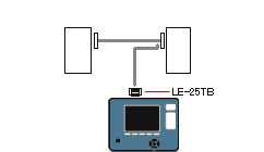
■RS-422/RS-485
Connect to RS-422/485 line as shown in the following figure by using the terminal block for DSUB 25-pin (LE-25TB) etc. of an option.
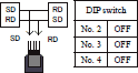
| Half-duplex | 2 (TxD_A), 14 (TxD_B) 7 Connect (GND) |
|---|---|
| Full-duplex | 2 (TxD_A), 14 (TxD_B) 3 (RxD_A), 16 (RxD_B) 7 Connect (GND) |
If you need the terminator, turn on by DIP SW on the interface board.
■TTL
Connect using the optional expansion kit "OP-SB85/OP-SB85L".
■HDLC Monitor
■HDLC Simulation
■SPI Monitor
■SPI Simulation
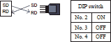
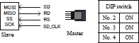
□Master Mode
Connect SDO(SD) to MOSI, SDI(RD) to MISO, SS(RTS) to SS, and SCK(TXC) to SCK.
■SPI Simulation
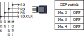
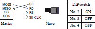
□Slave mode
Connect SDO(SD) to MOSI, SDI(RD) to MISO, SS(RTS) to SS, and SCK(TXC) to SCK.
Monitoring
It can monitor ASYNC/HDLC/Profibus-DP (Max 12Mbps) or SPI (Max 20Mbps) at arbitrary speed in real-time. Time stamp resolution that is effective to check the response time is selectable from 1mS/100uS/10uS/1uS. Therefore, it is useful for development and analysis of failures for High-speed communications effectively.
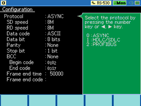
■ASYNC
ASYNC monitor function supports data bit length (7 or 8 bit), parity bit (none, even, or odd), and BCC (LRC-ODD/LRC-EVEN/CRC-16/CRC-ITU-T). With OP-SB85L, it can easily measure UART of microcomputer or communication module.
< ASYNC Setup Screen >
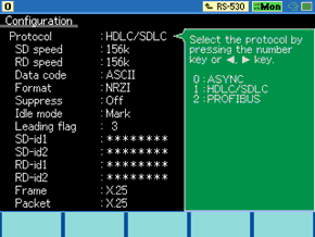
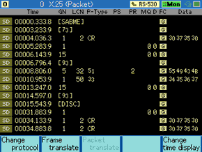
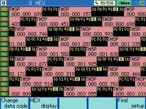
■HDLC/SDLC/X.25 and CC-Link
ID filter that can capture frames only on the specific address (16bits) can be individually specified on the SD and RD side. This improves the efficiency of analysis and data use in the capture memory. At the time of the half-duplex, the frames of specific address can be divided to the SD side, the other frames are sent to the RD side.
< HDLC Setup Screen >
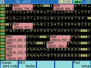
< HDLC Monitoring Screen (normal) >
< HDLC Monitoring Screen (frames) >
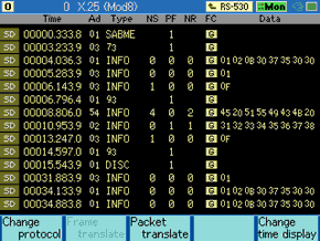
< HDLC Monitoring Screen (packets) >
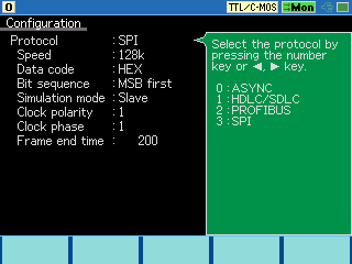
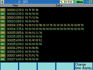
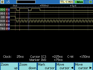
■SPI
There are 4 kinds of SPI transferring timing by clock polarity and clock phase.This products supports all these kinds and monitors SPI communications in most of the SPI devices. Some of the SPI devices transer all frames with low level SS signal. This product can analyze the relationship between transferring commands and data by setting the Frame End Time.
< SPI Setup Screen >
< SPI Monitoring Screen (normal) >
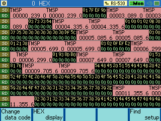
< SPI Monitoring Screen (dump) >
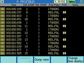
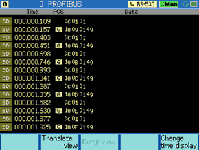
■Profibus-DP
It supports Profibus-DP (A high-speed fieldbus prevailing in the world). It takes frames out according to the communication standard of Profibus and you can see it in the translated display or execute error check of BCC.
< Profibus Monitoring Screen (normal) >
< Profibus Monitoring Screen (translate) >
< Profibus Monitoring Screen (dump) >
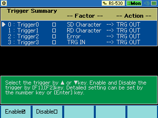
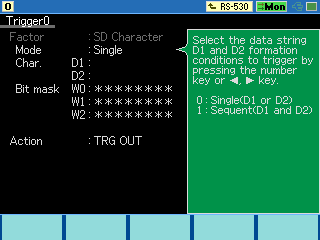
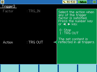
Trigger
It outputs a Low pulse to the external trigger terminal or automatically stops monitoring by single detection or sequential detection of two sets of characters (max 8 characters, you can choose don’t care and bit mask) or by detection of an error (CRC error, abort, short frame).
< Example of Trigger Setup Screen1 >
< Example of Trigger Setup Screen2 >
< Example of Trigger Setup Screen3 >
Simulation
Simulation function is useful when it is in the early stage of development, and when there are few partner devices to perform high-speed communications. By pressing the corresponded key, 16 kinds of data registered in the transmission data table can be transmitted once or repeatedly. For TTL interface, you can select the output signal level and type that suits to the target circuit. For SPI simulation, it has Master and Slave mode, and able to have the transmission/reception test up to 12Mbps (Master mode).
< SPI Setup Screen >
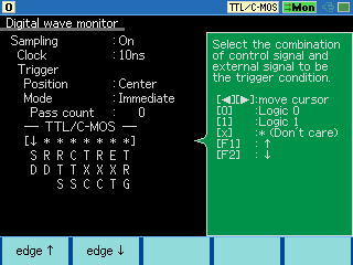
Support Logic Analyzer function (Ver.2.03 or later)
Logic Analyzer function at max 100MHz sampling speed enables you to analyze timing of high-speed HDLC and SPI signals by digital waveform. It helps you to solve the hardware troubles, and it is also useful for educational purpose for data communication studies.
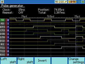
When the analyzer is LE-8200A, you can use pulse generator function with which you can edit and output a waveform.